Home
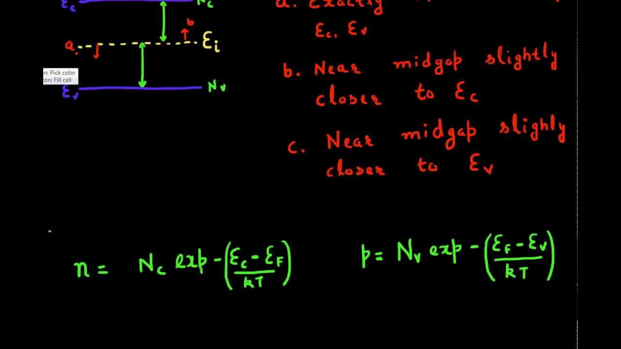
/ Fermi Level Expression In Intrinsic Semiconductor Is : 3: Schematic energy bands of different semiconductors. The ... / Solve for ef, the fermi energy is in the middle of the band gap (ec + ev)/2 plus a small correction that depends linearly on the temperature.
Fermi Level Expression In Intrinsic Semiconductor Is : 3: Schematic energy bands of different semiconductors. The ... / Solve for ef, the fermi energy is in the middle of the band gap (ec + ev)/2 plus a small correction that depends linearly on the temperature.
Fermi Level Expression In Intrinsic Semiconductor Is : 3: Schematic energy bands of different semiconductors. The ... / Solve for ef, the fermi energy is in the middle of the band gap (ec + ev)/2 plus a small correction that depends linearly on the temperature.. Densities of charge carriers in intrinsic semiconductors. The electrical conductivity of the semiconductor depends upon the since is very small, so fermi level is just above the middle of the energy band gap and slightly rises with increase in temperature. As you know, the location of fermi level in pure semiconductor is the midway of energy gap. The surface potential yrsis shown as positive (sze, 1981). Fermi level in intrinsic and extrinsic semiconductors.
Differentiate between intrinsic semiconductors and intrinsic semiconductors? Fermi level for intrinsic semiconductor. Therefore, the fermi level for the intrinsic semiconductor lies in the middle of forbidden band. The fermi level for an intrinsic semiconductor is obtained by equating (2.6) and (2.8) which yields. Fermi level in intrinsic and extrinsic semiconductors.
Position of Fermi level in instrinsic semiconductor - YouTube from i.ytimg.com Click hereto get an answer to your question fermi energy level for intrinsic semiconductors lies. An intrinsic semiconductor is an undoped semiconductor. For si, the intrinsic fermi level is calculated to be 0.54 ev above the valence band edge (ev) at room temperature. To be exact ef should be at the valence band edge (ev) at 0k because no energy state above ev are occupied at 0k; Distinction between conductors, semiconductor and insulators. Show transcribed image text 12.2 the effective mass of electrons at the lower conduction band edge of a semiconductor is three times higher than that of holes at the upper valence band edge. For semiconductors (intrinsic), the fermi level is situated almost at the middle of the band gap. The difference between an intrinsic semi.
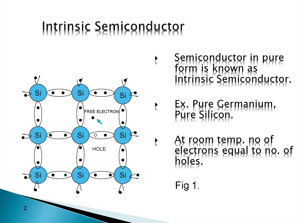
At absolute zero temperature intrinsic semiconductor acts as perfect insulator.
The surface potential yrsis shown as positive (sze, 1981). This level has equal probability of occupancy for the fermi level is the highest energy state occupied by electrons in a material at absolute zero temperature. Show transcribed image text 12.2 the effective mass of electrons at the lower conduction band edge of a semiconductor is three times higher than that of holes at the upper valence band edge. At absolute zero temperature intrinsic semiconductor acts. Www.studyleague.com 5 semiconductor fermilevel in intrinsic and extrinsic semiconductor theory. Fermi level in intrinic and extrinsic semiconductors. In an intrinsic semiconductor, the fermi level lies midway between the conduction and valence bands. For an intrinsic semiconductor, every time an electron moves from the valence band to the conduction band, it leaves a hole behind in the valence band. Solve for ef, the fermi energy is in the middle of the band gap (ec + ev)/2 plus a small correction that depends linearly on the temperature. Carefully refined semiconductors are called intrinsic semiconductors. Intrinsic semiconductors in an intrinsic semiconductor, all the electrons in the conduction band are thermally excited from the valence band. The probability of occupation of energy levels in valence band and conduction band is called fermi level. At absolute zero temperature intrinsic semiconductor acts as perfect insulator.
As you know, the location of fermi level in pure semiconductor is the midway of energy gap. The intrinsic fermi levelwith respect to the middle of the gap. Fermi level for intrinsic semiconductor. At absolute zero temperature intrinsic semiconductor acts as perfect insulator. Show transcribed image text 12.2 the effective mass of electrons at the lower conduction band edge of a semiconductor is three times higher than that of holes at the upper valence band edge.
Chapter2.2.3;2.2.4;2.2.5;Insulator,Semi-conductor,Metal ... from archive.cnx.org The energy intrinsic semiconductor is doped in order to increase conductivity of semiconductor. at any temperature t > 0k. At absolute zero temperature intrinsic semiconductor acts. The difference between an intrinsic semi. The fermi level for an intrinsic semiconductor is obtained by equating (2.6) and (2.8) which yields. Fermi level for intrinsic semiconductor. Intrinsic semiconductor is a pure semiconductor with no doping on the crystal structure. But in extrinsic semiconductor the position of fermil.
To be exact ef should be at the valence band edge (ev) at 0k because no energy state above ev are occupied at 0k;
For intrinsic semiconductors like silicon and germanium, the fermi level is essentially halfway between the valence and conduction bands. F (e) is the probability that a level with energy e will be filled by an electron, and the expression is:f (e) = 1 1. Doping increases majority charge carries either electrons or. (ii) fermi energy level : at any temperature t > 0k. The surface potential yrsis shown as positive (sze, 1981). Fermi level in intrinsic semiconductor. Densities of charge carriers in intrinsic semiconductors. There is an equal number of holes and electrons in an intrinsic material. An intrinsic semiconductor is an undoped semiconductor. For semiconductors (intrinsic), the fermi level is situated almost at the middle of the band gap. Show transcribed image text 12.2 the effective mass of electrons at the lower conduction band edge of a semiconductor is three times higher than that of holes at the upper valence band edge. In a silicon crystal each atom is surrounded by four neighbour atoms.
This picture is true for any intrinsic semiconductor, with the. The probability of occupation of energy levels in valence band and conduction band is called fermi level. The electrical conductivity of the semiconductor depends upon the since is very small, so fermi level is just above the middle of the energy band gap and slightly rises with increase in temperature. Fermi level for intrinsic semiconductor. Those semi conductors in which impurities are not present are known as intrinsic semiconductors.
Types of Semiconductors - презентация онлайн from cf2.ppt-online.org The intrinsic fermi levelwith respect to the middle of the gap. An intrinsic semiconductor is one which is made of the semiconductor material in its extremely pure. For si, the intrinsic fermi level is calculated to be 0.54 ev above the valence band edge (ev) at room temperature. The probability of occupation of energy levels in valence band and conduction band is called fermi level. As the temperature is increased, electrons start. Show transcribed image text 12.2 the effective mass of electrons at the lower conduction band edge of a semiconductor is three times higher than that of holes at the upper valence band edge. In a silicon crystal each atom is surrounded by four neighbour atoms. Fermi level in intrinic and extrinsic semiconductors.
Fermi level in intrinsic and extrinsic semiconductors.
Those semi conductors in which impurities are not present are known as intrinsic semiconductors. Show transcribed image text 12.2 the effective mass of electrons at the lower conduction band edge of a semiconductor is three times higher than that of holes at the upper valence band edge. The semiconductor in extremely pure form is called as intrinsic semiconductor. Where, nd = doping concentration. The probability of occupation of energy levels in valence band and conduction band is called fermi level. Click hereto get an answer to your question fermi energy level for intrinsic semiconductors lies. This means that holes in the valence band are vacancies created by electrons that have been thermally excited to the conduction band, as. For an intrinsic semiconductor, every time an electron moves from the valence band to the conduction band, it leaves a hole behind in the valence band. The number of charge carriers is therefore determined by the properties of the material itself instead of the amount of. Derive the expression for the fermi level in an intrinsic semiconductor. At absolute zero temperature intrinsic semiconductor acts as perfect insulator. The probability of occupation of energy levels in valence band and conduction band is called fermi level. For intrinsic semiconductors like silicon and germanium, the fermi level is essentially halfway between the valence and conduction bands.
Differentiate between intrinsic semiconductors and intrinsic semiconductors? fermi level in semiconductor. Fermi level in intrinsic and extrinsic semiconductors.

/2 plus a small correction that depends linearly on the temperature.)